Moving Message Display System
Introduction
This Moving Message Display System (MMDS) was one of the projects for A-Level electronics which I started in January 1997. What follows is more-or-less the original report for the project, and it explains the operation of the system and the design process for version 5 of the system.
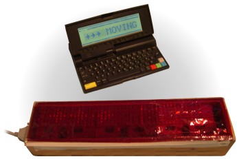
Version 6 of the MMDS with the
Amstrad NC200 Notebook computer
Later on, in version 6, I added to the design by allowing the system to be programmed from a computer via the parallel port, and increased the display size by using discrete LEDs on large display modules. Versions 5 and 6 were built on breadboard — although I did build the final circuit on a PCB, this failed to work correctly (possibly due to interference).
Specification
The aim of this project is to design a Moving Message Display System (MMDS) of the type commonly seen in shop windows, airports, and other public buildings.
- The display will be required to be able to scroll a message of at least 300 characters from right to left, with at least eight characters on screen at any instant.
- Other display features (such as flashing text) will not be needed, since it would be extremely difficult to add these using ordinary logic ICs.
- A dot-matrix style of LED display will be used that is capable of displaying the ASCII character set.
- An EPROM will be used to store the message initially, but if possible, a computer could be used to download data to a RAM via a parallel interface.
Principles of operation
Please refer to the block diagram of figure 1.
An EPROM is used to store the message to be displayed on the LED display. Bits D0 to D6 from the EPROM output correspond to the seven LEDs in one column of the display. A high output turns an LED on, the LED display being a common cathode type. The MSB, D7, is used to reset the system when the end of the message is reached; when it is high the system resets.
In order to scroll the message across the screen, the cathodes (display columns) of the LEDs are scanned by the Cathode Multiplex block at a speed high enough so that the flickering cannot be seen. As each column is selected, the corresponding data for the LED anodes (display rows) is output from the EPROM and the Main Address Counter is incremented.
After a number of scans set by the Scan Counter, the Base Address Counter is incremented and the new value loaded into the Main Address Counter. This sequence gives the illusion of the message scrolling across the display.
The system has a single clock which is effectively divided down by each block.
Complete block diagram
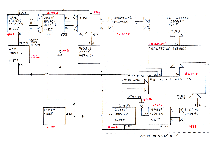
Figure 1: Complete block diagram
The LED display
The LED display could be made up of separate LEDs, but this would make producing a PCB difficult. Instead, I have used ready-made modules available from Rapid Electronics Ltd. These have 35 red LEDs arranged in a 5x7 matrix with the cathodes of each column and the anodes of each row commoned together, as shown in figure 2.
This results in there being 12 connections to each module, which makes producing a PCB easier.
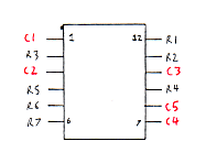
Figure 2: LED module pin-out
The number of modules required to give a good effect was decided by using the computer program in Appendix 1 which simulates on screen a message scrolling across a display.
Using this, I decided 16 modules would give a good display, allowing 13 characters to be shown on the display at any instant.
PCB
Rather than draw the copper pattern for the PCB by hand, since it is repetitive, I used a computer drawing package and a laser printer to produce an image on acetate film. Unfortunately, the number of display modules had to be reduced to 12 due to the size of the screen drawing area and the size of the UV light box used to produce the PCB.
With the PCB of figure 3, the first seven connections (marked in red) are the LED anodes, and the other 60 are the LED cathodes.
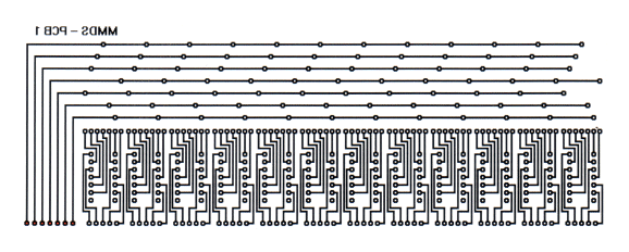
Figure 3: PCB copper track pattern
The EPROM
The characters in each message are stored in an EPROM with one byte corresponding to one column of dots. Storing the characters in this way rather than as their ASCII codes has the advantage that, apart from being simpler to decode with the electronics, any character or graphic needed can be easily formed.
The character definitions used in the system are those used in my NC200 computer, which uses a 5 x 8 matrix to display each character. Since the LED display modules are 5 x 7, only upper-case letters can be shown properly, since the letters ‘g’, ‘j’, ‘p’, ‘q’ and ‘y’ will lose their ‘tails’ (see figure 4).
An extra column is added between each character for spacing, meaning that each character is therefore 6x7.
The EPROM used in the system is the 2764, which has a storage capacity of 64K bits organized into 8,192 bytes. There are therefore thirteen address lines, which are split up, the first eleven (A0–A10) being set by the address counter block.
The number of address lines set by the address counter block determines the length of the message, meaning there are 2,048 (2 to the power of 11) columns available for a message. This means that the maximum length of each message is 341 characters (2,048 divided by 6), which satisfies the requirement of the specification.
|
|
|
|
|
|
|
|
|
|
|
|
|
|
|
|
|
|
|
|
|
|
|
|
|
|
|
|
|
|
|
|
|
|
|
The upper-case ‘A’ shown on a 5 x 7 matrix
|
|
|
|
|
|
|
|
|
|
|
|
|
|
|
|
|
|
|
|
|
|
|
|
|
|
|
|
|
|
|
|
|
|
|
|
|
|
|
|
|
The lower-case ‘y’ shown on a 5 x 8 matrix
|
Figure 4: Character definitions
Adding extra messages
The two extra address lines A11 and A12 are used to select one of four messages stored in the EPROM. Switches A and B select a message when set as shown below:
| Message |
Switch A |
Switch B |
| 1 |
Up |
Up |
| 2 |
Up |
Down |
| 3 |
Down |
Up |
| 4 |
Down |
Down |
Switches A and B are SPDT types connected as shown in figure 5 so that each address line is either connected to +5V or 0V.
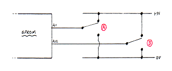
Figure 5: Switches A and B
Address counters
The address counters form the heart of the system as it is these that enable the scrolling of a message to take place. There are two counters which work together:
The Base address counter
The Base address counter is a 12-bit (only 11 bits are used) ripple counter IC (4040) which is reset to zero by bit D7 of the EPROM at the end of a message so that the first byte of data in a message is at the first EPROM address, 00000000000.
The counter then increments every time the Cathode Multiplex block finishes a scan, so that the display appears to scroll.
In the final design, the Scan Counter was added so that several scans of the display take place before the Base address counter is incremented.
The Main address counter
After the Base address counter is clocked at the beginning of a scan, a LOAD signal inputs the new address into the Main address counter. The Main address counter then advances from this address once each time the Cathode Multiplex block moves on to the next column.
The Main address counter needs to be 11 bits long and has to be programmable. Since this length of counter cannot be found in one IC package, three identical 4-bit programmable synchronous counters are used (74C161). These have common clock and common load lines, plus carry-in and carry-out pins which are connected as shown in figure 6.
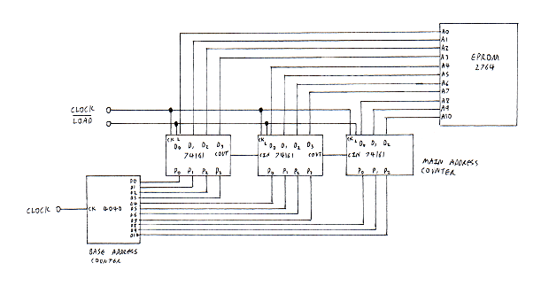
Figure 6: Address counters
The whole block was tested when built using two Logi-boxes to monitor the outputs and provide CK and LOAD inputs.
I noted that the 74C161 counters do not place data from their P0–P3 pins immediately onto their D0–D3 when LOAD is pulled low, but actually do this when the next CK pulse is recieved. This does not affect the operation of the circuit in any way.
Cathode Multiplex block
The function of this block is to pull one of sixty outputs low in order each time a clock pulse is received, i.e., a 1-of-60 decoder. Each of the outputs is connected to one column of LEDs on the display so that only one column can ever be on at any one time.
Since a 1-of-60 decoder is not available in one IC package, four 1-of-16 decoders (originally 4515) were used instead. However, this meant two extra counters and a 1-of-4 decoder were also needed. The circuit is shown in figure 7.

Figure 7: Cathode Multiplex block
Select counter
Each of the 1-of-16 decoders has 4 address lines, A to D. Connecting the Q0–Q3 outputs from a 4-bit counter (4520b) to each of the decoder address lines makes each decoder pull each of its outputs low in turn when the counter is clocked.
Now, all that is needed is a method to making only one decoder do this at a time.
Enable counter and decoder
The 1-of-16 decoders have an enable input, which, when brought low holds all their outputs high, thus preventing any display column to be on.
One output from a 1-of-4 decoder (4556a) is connected to each enable input so that only one 1-of-16 decoder is active at any one time.
The 1-of-4 decoder needs a 2-bit counter (4520a) to supply its address and this is clocked every time the D3 output of the Select counter returns to zero (i.e., when a count of 16 has been reached and the Select counter returns to 0000). Because the 4520 is positive clocked, a NOT gate is required to invert the D3 output before it clocks the Enable counter.
The block was then tested using a Logi-box to show the 4556 outputs changing and then applying the fast system clock and using 4 LED displays to check that scanning worked at high speed.
To do this the anodes of each row of LEDs were tied high. However, as more rows of LEDs were switched on, the LEDs became progressively dimmer due to the 4515 IC not being able to sink enough current.
In order for the LEDs to all be the same brightness I decided that the Anode Multiplex block was needed.
Anode Multiplex block
The Anode Multiplex block was designed to overcome the problem of the LEDs becoming dimmer by ensuring only one LED is on at any one time. (Note that this block was eventually taken out once transistor display drivers were added.)
The Anode Multiplex block scans each of the seven LEDs in a column in turn and either turns each one on or off depending on the data in the EPROM.
To do this, two 4051 8-input analogue multiplexers were used as shown in figure 8, with only 7 inputs/outputs being needed. Using analogue multiplexers means that data can flow to or from the switch ‘wiper’. For example, if address 010 is present on both multiplexer address lines, then data input to input 2 through the first multiplexer will be available on output 2 of the second multiplexer.
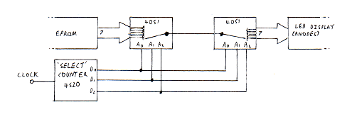
Figure 8: The analogue multiplexer ICs
Select counter
The Select counter is a 3-bit counter (4520) that provides the address inputs for the 4051 analogue multiplexers. The counter needs to count up to six, then reset on seven since there are seven LEDs in each column. This was achieved at first by using two AND gates wired as a three input AND as shown in figure 9[a]. However, when tested using a Logi-box, the counter reset on a count of four, rather than seven. This is because the signal is delayed in the first gate so that a glitch occurs when the output changes from 3 to 4, causing a brief reset signal to the counter, as shown in figure 10. To stop this, the inputs to the AND gates were swapped around as shown in figure 9[b].
![Figure 9: Resetting: [a] (A.B).C [b] (B.C).A Figure 9: Resetting: [a] (A.B).C [b] (B.C).A](/items/moving-message-display-system/figure-9.gif)
Figure 9: Resetting: [a] (A.B).C [b] (B.C).A
| C |
B |
A |
Reset |
Notes |
| 0 |
0 |
0 |
0 |
|
| 0 |
0 |
1 |
0 |
|
| 0 |
1 |
0 |
0 |
|
| 0 |
1 |
1 |
0 |
|
| 1 |
0 |
0 |
1 |
Incorrect reset |
| 1 |
0 |
1 |
0 |
|
| 1 |
1 |
0 |
0 |
|
| 1 |
1 |
1 |
0 |
Reset should occur here |
Figure 10: Counter truth table with incorrect reset
System clock
The system clock is produced by a NE555 astable circuit as shown in figure 11.
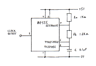
Figure 11: System clock
The frequency of the astable was at first based on the scan rate of a TV screen, 25Hz, because at this frequency the screen cannot be seen to flicker.
The clock frequency of the display system was therefore chosen to be 1.5kHz (25Hz x 60), since there are 60 LEDs in the display.
The formula for the frequency of an NE555 astable is:

Therefore:

If Ra is chosen to be 1kΩ and C is chosen to 0.1μF, then:

With this value, the scanning of the display could still be seen (possibly because LEDs have a lower persistence than the phosphor in a TV screen), and the value was finally changed to 1.6kΩ giving:

Connecting the blocks together
When the system was first connected up as shown in figure 12, a slower system clock was used for testing, and the Cathode and Anode Multiplex blocks were seen to function together correctly. However, the Main address counter did not count due to the length of the Anode Multiplex block Select counter reset pulse not being enough to clock the counter. This problem was solved by placing two spare NOT gates at the reset input of the Select counter and connecting their output to the clock input of the Main address counter, as shown in figure 13. Another problem to be sorted out was that the the Main address counter did not load in it’s new value from the Base address counter at the end of each scan. Again, this was due to the short length of the Cathode Multiplex block reset pulse.
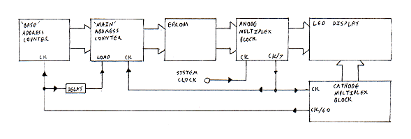
Figure 12: Original design for system
Using the spare outputs
The problem was solved by re-designing the resetting of the system.
Since there are 60 columns of LEDs used in the system, there are 4 spare outputs from one of the 1-of-16 decoders, each one being taken high when it is selected, and they are selected one at a time by the Cathode Multiplex block. I decided to use three of these to do the following tasks:
- Clock the Base address counter. The length of the pulse means the counter has time to settle into its new state before the Main address counter loads in the new value.
- Load in the new value of the Base address into the Main address counter.
- Reset the Cathode Multiplex block since there is one output still left unused.
When tried, it was found that the Base address counter was being clocked twice each time output 61 went high due to a glitch. When a logic probe or an oscilloscope was connected to output 61 to try to observe the glitch, it disappeared. This must have been because of the load placed on the output by the test instruments, so I placed a variety of resistances between the output and +5V to try to stop the glitch. When this failed, I tried a 0.2nF capacitor (equal to the capacitance of the oscilloscope) instead cured the problem. After this, the design worked perfectly because the clock and load pulses are now longer, guaranteeing that the Base counter will be clocked and the Main counter will load in the new value from the Base counter.

Figure 13: Using NOT gates to delay the pulse
De-coupling capacitors
Six 0.1μF capacitors were placed near to many of the ICs to avoid problems with glitches causing unwanted clocking, etc. (The circuit behaved erratically when capacitors near the 555 IC were removed.)
Larger 100μF capacitors were also placed on each breadboard to smooth the power supply.
Display drivers
The brightness of the LED display was not adequate due to the small amount of current (25mA) that could be sourced from the 4051 and sunk into the 4515 ICs. At a high scan rate, the LEDs appear dimmer even with 25mA through them.
So that higher currents could be supplied to the LEDs, two types of transistor drivers were used, placed as shown in figure 14.
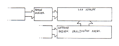
Figure 14: Positioning of display drivers
Darlington pairs
Nine ULN2004 ICs were used at the LED cathodes to sink the higher current. Each IC has seven identical Darlington Pair drivers as shown in figure 15. These can sink a maximum of 550mA, so are perfect for this application.
However, the Darlington Pairs are inverting, meaning that the 4515 ICs needed to be swapped for 4514 ICs (they both have the same pinout!) so that bringing an output high allows a column of LEDs to be switched on, since the output of the corresponding Darlington Pair will become low.
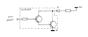
Figure 15: ULN2004 Darlington driver IC
Transistor drivers
For the LED anodes, the ULN2004 could not be used since current needs to be sourced from the driver circuit rather than sunk. Therefore, the transistor switch circuit shown in figure 16 was used. When the base voltage is 5V, the transistor is fully switched on, allowing a larger current to flow through the transistor into the LED.
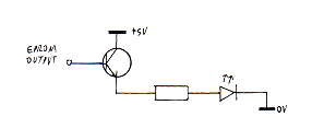
Figure 16: Transistor driver
LED resistors
Because of the transistor driver, 0.7V is lost from the 5V supply, meaning that there is 4.3V across the LED and resistor. Because the display is being scanned at high speed, the LEDs are only on for a brief period, meaning that they will appear dim unless a higher current than they would normally use is pushed through them. The low resistance of 47Ω gave a bright display, meaning that the current through the LEDs is 90mA.
Because the brightness of the display does not now depend on the amount of current the ICs can sink and source, the Anode Multiplex block was removed, cutting down the number of ICs in the system from 27 to 23.
Scan counter
The scan counter was added so that the speed of scrolling could be altered. The counter is a 4-bit 4520 counter that simply divides it's clock input down by 2, 4, 8 or 16 depending on which Q output is used. Therefore, if output Q3 is connected, the display will be scanned eight times before the Base address counter is incremented.

Figure 17: Scan counter
Programming by computer
A requirement of the specification was that the system could be programmed by computer. Unfortunately, I did not have time to build and test the additions to the existing circuit described below.
The simplified block diagram of figure 18 shows how the computer interface could have been added.
The EPROM would be exchanged for a Random Access Memory of the same memory capacity. Using the parallel port of a computer such as the BBC Micro, each byte of data would be downloaded in order, the STROBE output acting as a clock for the Main address counter. A tri-state device such as the 74254 would allow the data to be entered into the RAM. Before commencing downloading, a switch S3 in the circuit would need to be moved to get the system ready to accept the new data by ensuring the following:
- That the Main address counter is reset to zero.
- The system clock is disabled and the STROBE is routed to the Main address counter clock.
- The RAM is set to write mode.
- The correct set of tri-state buffers is enabled.
Handshaking with the computer could be done by mimicking a printer’s response to the new data using two monostable timers to provide the ACK and BUSY outputs (as in the ‘Parallel Interface Relay Card’ article; see References).
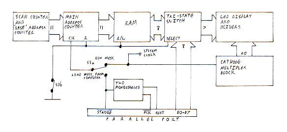
Figure 18: Computer interface
Full circuit diagram (version 5)
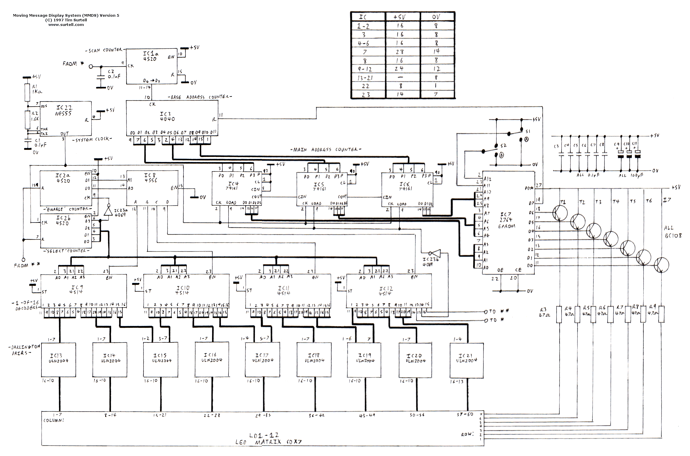
Figure 19: Full circuit diagram (version 5) — Click to enlarge
Parts list (version 5)
| Reference(s) |
Part |
Quantity |
| R1 |
10kΩ 0.25W carbon film resistor |
1 |
| R2 |
1.6kΩ 0.25W carbon film resistor |
1 |
| R3–R9 |
47Ω 0.25W carbon film resistor |
8 |
| C1, C3–C8 |
0.1µF 25V ceramic disc capacitor |
8 |
| C2 |
0.1nF 25V ceramic disc capacitor |
1 |
| C9–C11 |
100µF 16V electrolytic capacitor |
3 |
| T1–T7 |
BC108C 25V NPN transistor |
7 |
| IC1, IC2 |
4520 dual 4-bit binary synchonous counter |
2 |
| IC3 |
4040 12-bit binary ripple counter |
1 |
| IC4–IC6 |
74161 4-bit binary programmable synchonous counter |
3 |
| IC7 |
2764 64K EPROM |
1 |
| IC8 |
4556 dual 1-of-4 decoder |
1 |
| IC9–IC12 |
4514 1-of-16 decoder |
4 |
| IC13–IC21 |
ULN2004 Darlington transistor array |
9 |
| IC22 |
555 timer |
1 |
| IC23 |
4069 hex inverter |
1 |
| LD1–LD12 |
5 x 7 red LED matrix |
12 |
| S1, S2 |
SPDT toggle switch |
2 |
Conclusion
Apart from not having a computer interface, the system satisfies the specification. It has a display which is 60 columns wide, enabling 10 characters to be shown at any one time. The maximum length of each message is 628 characters because the 12-bit counter gives a maximum count of 4,096. By adding extra counters a message length of 1,365 could be achieved using the 2764 EPROM.
The Message Select switches were added to enable up to four individual messages to be stored on the same EPROM. This is a feature which could be excluded should a computer interface be added.
An extra counter, the Scan Counter, was added to enable the scrolling rate of the message to be changed from a slow crawl to a smooth ‘glide’ across the display.
The circuit runs from a 5V DC regulated supply and consumes around 300mA peak when at LEDs are lit.
Although it does not have some of the special effects that commercial display systems do, this system is considerably cheaper to produce, costing about £45, compared to a typical commercial system costing around £200.
One problem with the system is that the display brightness needs increasing further so it can be seen in bright artificial light and sun light.
If standard 5mm LEDs were used instead of 5 x 7 matrices the display could be made ½m long instead of 16cm, and yet the system would cost less — only £30!
Suggested additions to the circuit
- Two rows: To enable lower-case letters to be shown properly, the display could be doubled in size to 14 dots in a column. This would also allow different sizes and styles of writing to be used, and better graphics to be produced. It should be fairly easy to add an extra row if a block similar to the Anode Multiplexing block were introduced to run each row alternately. The message length would of course be halved, two bytes of data being needed for each column (figure 20).
- Pause: If two bytes for each column were used (as above), there would be two spare bits. One would still be used for resetting, but the other could be used for an effect such as pausing the display. Pausing can be already achieved if the clock pulse to the Base address counter is stopped. The extra bit could trigger a monostable to cut off the clock signal (figure 21).
- Dual or full-colour display: The same technique as used to create two display rows could also be used for a dual-colour or full-colour display.

Figure 20: Two row display — simplified block diagram
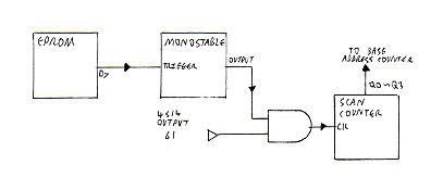
Figure 21: Pausing the display — simplified block diagram
Additions to the circuit (version 6)
After my A-Levels were finished, I did some more work on the MMDS, as briefly summarised below:
The display module PCBs
Using Microsoft Paint I designed a PCB that could accommodate a matrix of 16 x 7 standard 5mm LEDs spaced 1cm apart.
This PCB includes two ULN2803 darlington pair ICs and one 4514 1-of-16 decoder IC. Up to four PCBs can be arranged side-by-side to create a large display.
Programming by computer
In order to program messages into the system, the EPROM was replaced with a RAM and tri-state buffers to control the data flow. The RAM has a rechargeable backup battery. A ‘run/program’ switch sets up the system to either run the selected message or wait for bytes received on the parallel port. A circuit from Electronics — the Maplin Magazine was used to simulate the responses a printer would make to a PC on the parallel port.
Messages are written using the MMDS Editor software which I wrote for the Amstrad NC200 Notebook computer.
Full circuit diagram (version 6)
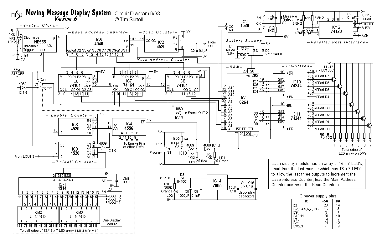
Figure 22: Full circuit diagram (version 6) — Click to enlarge
Parts list (version 6)
| Reference(s) |
Part |
Quantity |
| R1, R4 |
10kΩ 0.25W carbon film resistor |
2 |
| R2, R3, R12 |
1kΩ 0.25W carbon film resistor |
3 |
| R5–R11 |
10Ω 0.25W carbon film resistor |
7 |
| R13 |
750Ω 0.25W carbon film resistor |
1 |
| R14, R15 |
6.8kΩ 0.25W carbon film resistor |
2 |
| R16 |
360Ω 0.25W carbon film resistor |
1 |
| VR1 |
10kΩ linear potentiometer |
1 |
| C1, C2, C7, C9, C11–C16 |
0.1µF 25V ceramic disc capacitor |
10 |
| C3 |
100µF 16V electrolytic capacitor |
1 |
| C4 |
1µF 16V electrolytic capacitor |
1 |
| C5, C6 |
4.7µF 16V electrolytic capacitor |
2 |
| C8 |
1000µF 16V electrolytic capacitor |
1 |
| C10 |
10µF 16V electrolytic capacitor |
1 |
| CM1 |
0.1µF 25V ceramic disc capacitor |
1* |
| T1–T7 |
BC108C 25V NPN transistor |
7 |
| D1–D3 |
1N4001 1A rectifier diode |
3 |
| IC1 |
6264 64K static RAM |
1 |
| IC2, IC3 |
4520 dual 4-bit binary synchonous counter |
2 |
| IC4 |
4556 dual 1-of-4 decoder |
1 |
| IC5 |
4040 12-bit binary ripple counter |
1 |
| IC6–IC8 |
74161 4-bit binary programmable synchonous counter |
3 |
| IC9 |
555 timer |
1 |
| IC10, IC11 |
74244 octal tri-state buffer |
2 |
| IC12 |
74123 dual retriggerable monostable multivibrator |
1 |
| IC13 |
4069 hex inverter |
1 |
| IC14 |
7805 5V 1A voltage regulator |
1 |
| ICM1 |
4514 1-of-16 decoder |
1* |
| ICM2, ICM3 |
ULN2803 Darlington transistor array |
2* |
| LD1 |
5mm red/green bi-colour LED |
1 |
| LD2 |
5mm orange LED |
1 |
| LM1–91/112 |
5mm red LED |
91/112* |
| B1 |
3.6V NicCad battery |
1 |
| CN1 |
Parallel port connector |
1 |
| S1 |
DPDT toggle switch |
1 |
| S2 |
Push-to-make button |
1 |
* Per display module — see note on circuit diagram
Appendices
Appendix 1: Moving Message Display Simulator program
The following software was written in BBC BASIC for the Amstrad Notebook NC200 so as to judge the size of display needed to give a good effect.
 10 REM MMDS Simulator program
 20 REM Programmed by Tim Surtell
 30 :
 40 mess$="Moving Message Display System"
 50 delay=15
 60 dlen=12
 70 mess$=STRING$(dlen," ")+mess$+STRING$(dlen," ")
 80 :
 90 CLS
100 FOR I=1 TO LEN(mess$)
110 PRINT TAB(1,1)MID$(mess$,I,dlen)
120 TIME=0:REPEAT UNTIL TIME>delay
130 NEXT
140 GOTO 100
Note that the real display system scrolls column by column, not character by character.
Appendix 2: EPROM data program
This program was written in BBC BASIC for the BBC Micro by John Hewes to allow a message stored in the ‘M$’ variable to be viewed on the screen and printed as it will appear on the LED display. The resulting list of bytes can then be dumped to the EPROM programmer.
Please note that character definitions are given for the supplied test message only.
  10 REM EPROM data program
  20 REM Programmed by J. Hewes
  30 REM *** Warning! Do not use RENUMBER (due to DATA statements)
  40 :
  50 MODE 0
  60 DIM M% 1000
  70 :
  80 M$=STRING$(16," ")+">>> MOVING MESSAGE DISPLAY SYSTEM >>>"+STRING$(16,"*")+"@"
  90 :
 100 IF LEN(M$)>1000DIV6 PRINT "Message too long!":END
 110 :
 120 FOR I%=1 TO LEN(M$)
 130 C%=ASC(MID$(M$,I%)):VDUC%
 140 RESTORE C%+1000
 150 FOR N%=0 TO 5:READ B%:?(M%+6*I%+N%-6)=B%:NEXT
 160 NEXT
 170 :
 180 REM Check on screen
 190 :
 200 FOR I%=0 TO 6*LEN(M$)
 210 IF ?(M%+I%)=0 GOTO 260
 220 X%=2*I%:Y%=40
 230 FOR B%=0 TO 7
 240 IF ((?(M%+I%))AND2^B%)>0 PLOT69,X%,Y%+4*B%
 250 NEXT
 260 NEXT
 270 :
 280 PRINT "Print ? (Y/N)":IF GET$<>"Y" END
 290 :
 300 REM Check on printer
 310 :
 320 VDU 2:PRINT M$
 330 VDU 1,27,1,42,1,1,1,(6*LEN(M$))MOD256,1,(6*LEN(M$))DIV256
 340 FOR I%=0 TO 6*LEN(M$)
 350 VDU 1,?(M%+I%)
 360 NEXT
 370 VDU 3
 380 END
 390 :
1000 REM Character data (Line No. = 1000 + ASCII code)
1032 DATA 0,0,0,0,0,0 :REM Space
1042 DATA 127,127,127,127,127,127 :REM Block (*)
1062 DATA 0,8,8,62,28,8 :REM Right arrow (>)
1064 DATA 128,128,128,128,128,128 :REM End marker (@)
1065 DATA 0,63,68,68,68,63 :REM A
1066 DATA 0,127,73,73,73,54 :REM B
1068 DATA 0,127,65,65,65,62 :REM D
1069 DATA 0,127,73,73,73,65 :REM E
1071 DATA 0,62,65,65,69,127 :REM G
1072 DATA 0,127,8,8,8,127 :REM H
1073 DATA 0,0,65,127,65,0 :REM I
1076 DATA 0,127,1,1,1,1, :REM L
1077 DATA 0,127,32,16,32,127 :REM M
1078 DATA 0,127,16,8,4,127 :REM N
1079 DATA 0,62,65,65,65,62 :REM O
1080 DATA 0,127,72,72,72,48 :REM P
1082 DATA 0,127,72,76,74,49 :REM R
1083 DATA 0,50,73,73,73,38 :REM S
1084 DATA 0,64,64,127,64,64 :REM T
1085 DATA 0,126,1,1,1,126 :REM U
1086 DATA 0,112,12,3,12,112 :REM V
1089 DATA 0,96,16,15,16,96 :REM Y
Appendix 3: Test messages
Four test messages are available to download and can be read by the MMDS Editor software.
Photographs of the completed project
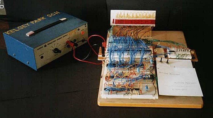
Version 5 built on breadboard
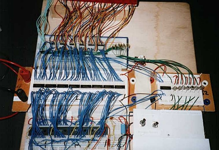
Version 5 built on breadboard (close-up)
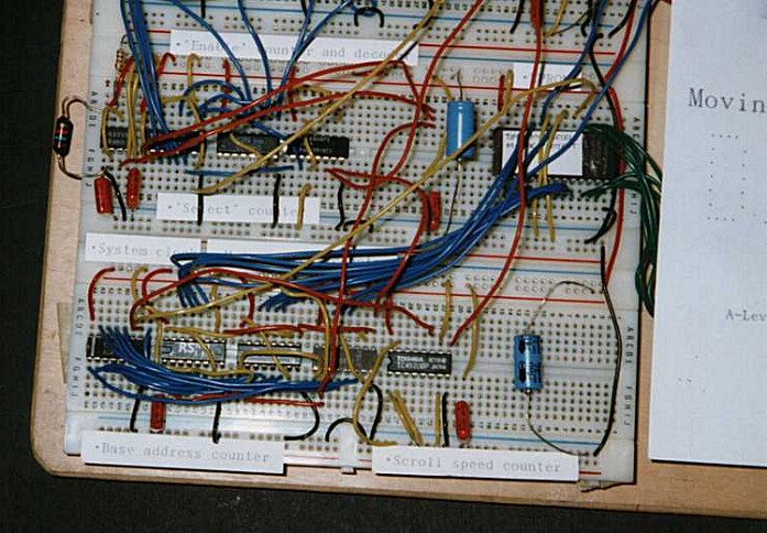
Version 5 built on breadboard (close-up)
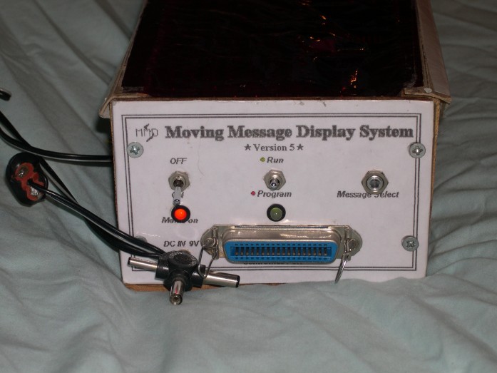
Version 6 case side panel
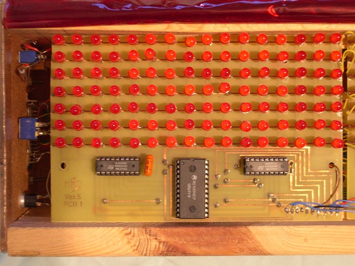
One of the version 6 display modules
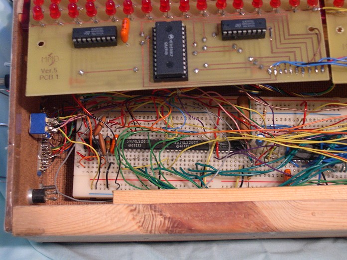
Version 6 built on breadboard (close-up)
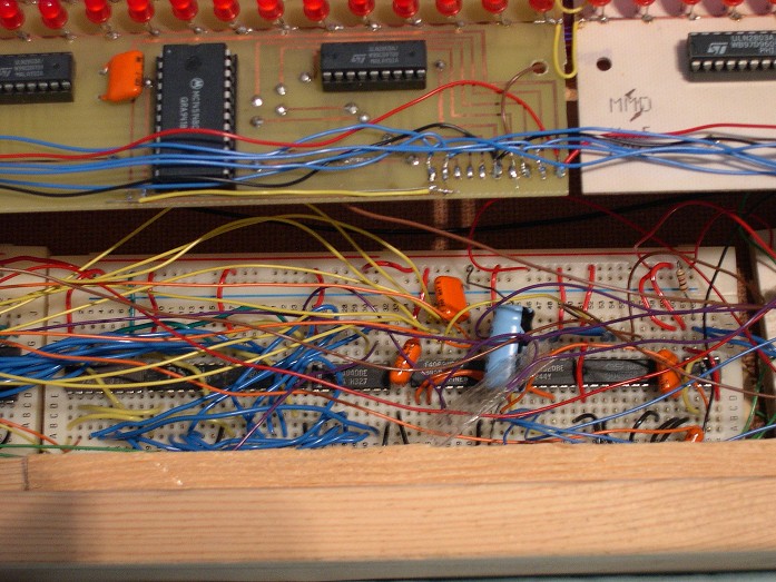
Version 6 built on breadboard (close-up)
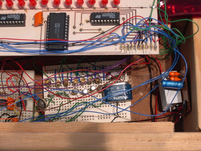
Version 6 built on breadboard (close-up)
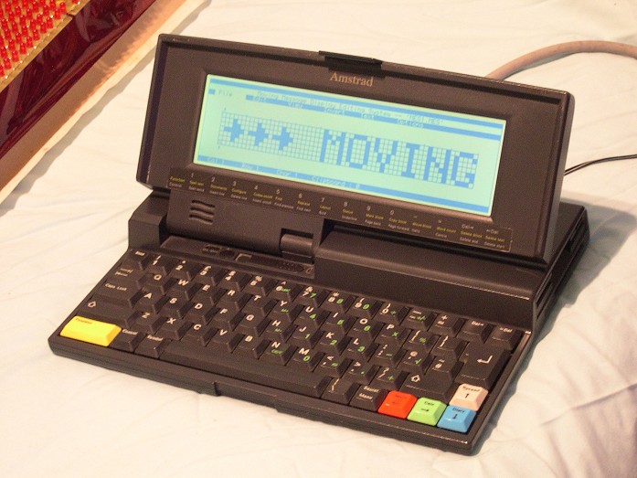
The Amstrad NC200 Notebook computer running the MMDS Editor software
References
- Lancaster, D., 1989, CMOS Cookbook
- Mullard ICs, 1985, CMOS Digital ICs, Book 4/Part 4
- Rapid Electronics Ltd., 1996–1997 Catalogue
- RS Ltd., 1996 Catalogue
- Ford, N., Parallel Interface Relay Card, Electronics — The Maplin Magazine, Issue 57
- Penfold, R., Interface, Everyday Practical Electronics, Volume 26/Issue 2
Thank you to John Hewes for programming the EPROM for me and writing the software in Appendix 2.